Description
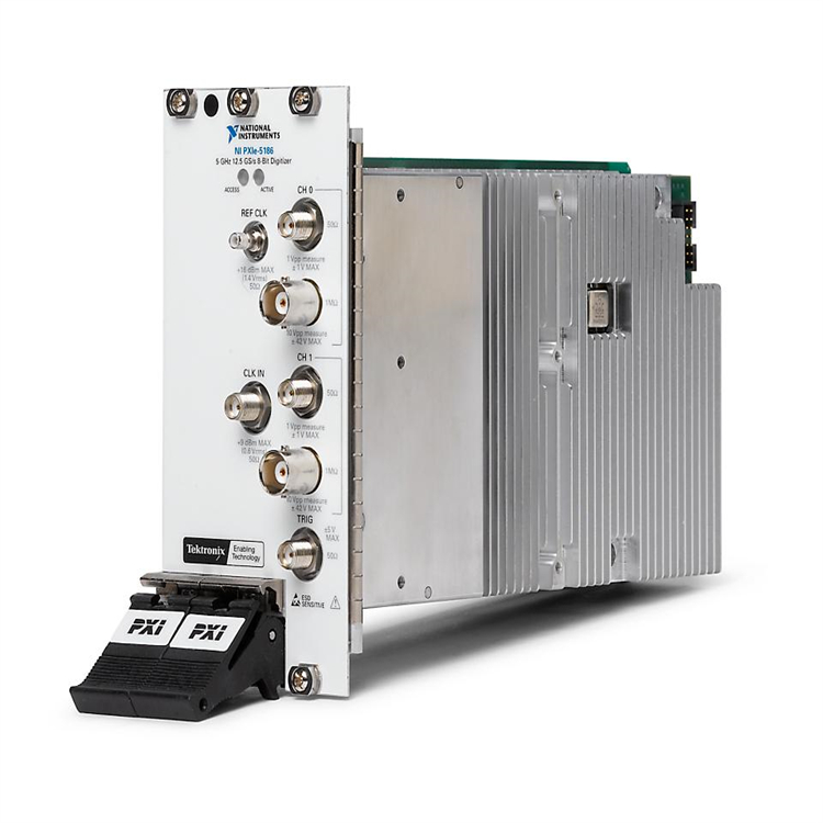
NI PXLE-5186 782058-02
1. Basic Information
Model: PXIe-5186
Part Number: 782058-02
Brand: NI (National Instruments)
Supported Platform: PXI Express modular test and measurement bus platform, compatible with the full series of PXIe chassisProduct Type: Single-slot high-speed 8-bit digitizing oscilloscope module. It features 2-channel 5 GHz wideband RF acquisition, a maximum real-time sampling rate of 12.5 GS/s, and large-capacity 1 GB onboard memory. Designed for high-speed digital, RF, millimeter-wave and high-speed serial bus signal acquisition, it supports nanosecond-level multi-module synchronous triggering and continuous streaming upload of massive data streams.
Product Positioning
Model 782058-02 is the standard hardware version of the PXIe-5186, with three core capabilities: 5 GHz analog bandwidth, dual-channel synchronous acquisition, 12.5 GS/s real-time sampling, and 1 GB per-channel deep onboard memory. It can accurately capture high-frequency transient waveforms such as high-speed clock signals, high-speed serial signals, RF pulses, transient electromagnetic interference and millimeter-wave modulated signals. It supports flexible switching between two input impedances (50 Ω / 1 MΩ) and programmable AC/DC coupling configuration, and integrates more than ten advanced triggering modes including edge, pulse width, video, window and sequence triggering.
Hardware Architecture
5 GHz Wideband RF Front-End Signal Conditioning Unit
Two independent RF signal channels are integrated, each equipped with a programmable impedance switching circuit (50 Ω RF matching / 1 MΩ general high impedance), AC/DC coupling switch, multi-stage programmable gain amplifier and hardware anti-aliasing filter. With a VSWR ≤ 1.25, it effectively suppresses high-frequency signal reflection and harmonic interference, ensures accurate amplitude and phase acquisition across the full bandwidth, and delivers a rise time as low as 170 ps.
12.5 GS/s High-Speed 8-bit ADC Sampling Unit
1 GB Per-Channel Deep Onboard Storage Unit
Each channel is equipped with 1 GB high-speed acquisition memory, supporting segmented acquisition, sequence triggering and segmented storage of ultra-long waveforms. It can capture a single ultra-long transient waveform or store tens of thousands of pulse event waveforms in batches, addressing common testing pain points including difficulty in reproducing intermittent high-frequency fault signals and data loss.
Multi-Mode Hardware Trigger & Timing Synchronization Unit
Built-in High-Precision Self-Calibration Signal Source Unit
An on-board high-stability DC reference calibration source enables one-click full-channel self-calibration for gain, offset, impedance and bandwidth to automatically compensate measurement drift caused by ambient temperature variations. The factory calibration is valid for one year, which significantly reduces on-site periodic external calibration and maintenance costs and guarantees stable measurement accuracy under wide-temperature operating conditions.
PCIe Gen3 High-Speed Bus Data Transmission Unit
Mounting Specifications
- Mounting Method: Embedded installation into a standard 3U single-slot PXIe chassis, compatible with the full series of PXIe chassis including PXIe-1085, supporting in-situ replacement in any slot
- Form Factor: Standard 3U PXIe card size with integrated aluminum heat sinks
- Front Panel Interfaces: 2 BNC analog input channels, 1 SMB external sampling clock input, 1 SMB reference clock input, multiple PFI trigger terminals, LED indicators for hardware status
- Driver Software: Official NI-SCOPE driver, compatible with NI MAX, LabVIEW, TestStand, Python, C# and other development tools
- Firmware Compatibility: Backward compatible with all PXIe chassis backplanes; supports Windows desktop OS and NI Linux Real-Time OS; can be synchronously networked with any NI oscilloscope or signal generator on the same platform
Supporting System
Supporting Hardware
Commissioning Tools
Upper-Level System Integration
Typical Application Industries
Product Features
1. 5 GHz Ultra-Wide Bandwidth + 12.5 GS/s Real-Time Sampling for Accurate High-Frequency Signal Restoration
2. 1 GB Large-Capacity Deep Onboard Memory for Reliable Intermittent Fault Waveform Capture
3. Dual-Impedance Design for Flexible Compatibility with RF and General Electrical Signals
4. Built-In Hardware Self-Calibration Ensures Long-Term Measurement Stability Under Wide-Temperature Conditions
5. Sub-10 ps Multi-Module High-Precision Synchronization for Distributed Large-Scale Test Networking
6. High-Speed Hardware Streaming Data Transmission for Long-Term Lossless Continuous Acquisition
2. Technical Specifications
2.1 Core Analog Input Parameters
- Number of Channels: 2 independent synchronous analog input channels
- Analog Bandwidth: 5 GHz @ 50 Ω; 500 MHz @ 1 MΩ
- Real-Time Sampling Rate: Max. 12.5 GS/s (single channel); 6.25 GS/s per channel (dual-channel synchronous mode)
- Sampling Resolution: 8-bit ADC
- Typical Rise Time: 170 ps (50 Ω bandwidth mode)
- Selectable Input Impedance (Software Configurable): 50 Ω / 1 MΩ, VSWR ≤ 1.25
- Coupling Mode: Programmable AC coupling / DC coupling
- Full-Scale Voltage Range @ 50 Ω: 0.05 ~ 5 V peak-to-peak
- Full-Scale Voltage Range @ 1 MΩ: 0.05 ~ 50 V peak-to-peak
- Maximum Safe Input Voltage: 3 Vrms (50 Ω mode); 50 Vrms (1 MΩ mode)
2.2 Memory & Trigger Parameters
- Onboard Memory Capacity: 1 GB deep memory per channel
- Trigger Types: Edge, glitch, pulse width, runt, window, video, sequence, external hardware trigger, bus protocol trigger
- Typical Trigger Jitter: < 15 ps RMS
- Trigger Sensitivity: 3% of full scale
- External Reference Clock: 10 MHz / 100 MHz SMB input; external sampling clock 1.6~3.125 GHz SMA input
- Synchronization Methods: PXIe backplane clock, RTSI synchronization bus, phase-locked synchronization via external high-precision reference clock
2.3 Bus & Communication Parameters
- Bus Standard: PXI Express Gen3, 8 GB/s unidirectional bandwidth per slot
- Data Transmission Modes: Hardware DMA streaming continuous upload, segmented acquisition via single trigger
- Driver Architecture: NI-SCOPE, compatible with Windows and NI Real-Time OS
- Timing Synchronization Accuracy Between Multiple Modules: < 10 ps
2.4 Environmental Specifications
- Operating Temperature: 0 ℃ ~ +55 ℃ (chassis air-cooled full-load condition)
- Storage & Transportation Temperature: -20 ℃ ~ +70 ℃
- Relative Humidity During Operation: 10% ~ 80% RH, non-condensing, free of corrosive gas and conductive dust
- Vibration Compliance: IEC 60068-2-6, continuous vibration resistance of 0.3 grms within 5~500 Hz
- MTBF (Mean Time Between Failures): ≥ 250,000 hours
- Ingress Protection Rating: IP20, to be installed only in sealed dust-proof shielded industrial control cabinets
2.5 Mechanical & Physical Specifications
- Mounting Method: Fixed installation in a 3U single-slot PXIe chassis with panel locking screws
- Net Weight: Approximately 1.15 kg
- Housing Structure: Reinforced shielded aluminum enclosure with integrated heat sinks; PCB coated with three-proof material
- Front Panel Configuration: 2 BNC analog input ports, SMB reference clock port, SMA external sampling clock port, PFI trigger terminals, four LED status indicators for Power / Run / Trigger / Overload
3. Key Features
Large Deep Memory Enables Locked Capture of Intermittent Fault Waveforms
Combining 1 GB onboard memory with multiple intelligent trigger modes, the module monitors random abnormal waveforms for long durations and automatically filters and stores fault segments, resolving testing challenges caused by hard-to-reproduce intermittent electromagnetic interference and sporadic hardware failures.Dual-Impedance and Dual-Coupling Modes Cover RF and General Electrical Testing
The 50 Ω impedance with AC coupling suppresses DC offset for RF R&D applications, while 1 MΩ high impedance with DC direct sampling is adopted for general industrial voltage and low-frequency sensor testing. One single module supports diverse test scenarios and reduces hardware investment.One-Click Hardware Self-Calibration Ensures Stable Measurement Accuracy Under Wide Temperature
An on-chip high-precision reference source automatically calibrates full-channel gain, offset and bandwidth to eliminate temperature-induced measurement errors, eliminating frequent manual external calibration and ensuring consistent test results in mass production.Sub-10 ps Multi-Device Synchronization Enables Distributed Test System Construction
With external high-precision clocks and the RTSI synchronization bus, multiple oscilloscopes and signal generators achieve strict timing synchronization to build multi-channel RF arrays and multi-node distributed synchronous automated test platforms.High-Speed Streaming Data Transmission Supports Long-Term Uninterrupted Monitoring
PCIe Gen3 hardware DMA streaming upload realizes lossless real-time storage of massive waveforms, supporting round-the-clock equipment reliability aging tests, long-duration continuous electromagnetic environment monitoring and full-lifecycle fault waveform traceability analysis.4. Working Principle
5. Application Scenarios
- High-Speed Communications & Semiconductor Industry: Signal integrity testing for high-speed serial buses such as PCIe, USB and Ethernet; eye diagram, jitter and rising-edge parameter acquisition and verification for chip high-speed IO interfaces.
- Automotive Electronics & Millimeter-Wave Radar: Waveform acquisition for transmit and receive signals of 77 GHz automotive radars, automated testing of modulated signal parameters and pulse timing sequences.
- Aerospace & Military Testing: Waveform capture for airborne radar and navigation RF equipment, transient EMC interference testing, and timing consistency verification for pulse commands.
- Power & New Energy Industry: Transient voltage and current waveform acquisition for IGBT and SiC power devices; capture and analysis of overshoot, oscillation and spike fault waveforms.
- Automated Test System Renovation Projects: Replacement and upgrade of legacy low-bandwidth oscilloscope modules to build high-frequency RF automated test platforms, reusing existing PXIe chassis and test programs to reduce hardware renovation costs.