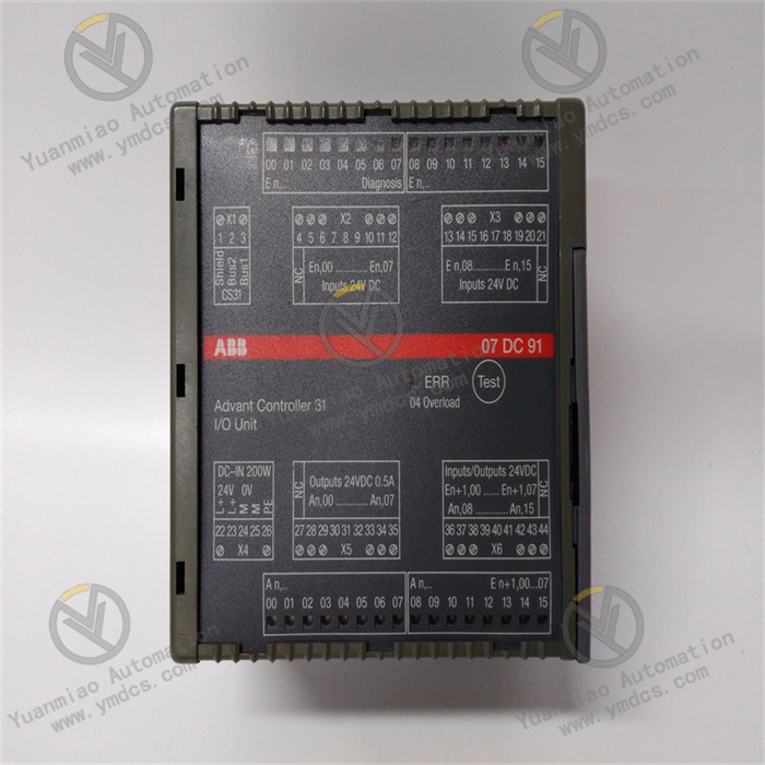
Description
1. Product Overview
LAM 685‑069171‑100 is an original‑equipment ultra‑high‑precision linear displacement encoder manufactured by Lam Research of the United States. Developed for semiconductor wafer processing, precision micro‑electronics manufacturing and displacement‑monitoring scenarios of high‑end precision equipment, it serves as a core precision‑measurement spare part for semiconductor tools. As the core component for equipment displacement feedback and position closed‑loop control, this encoder acquires real‑time high‑accuracy data of linear travel position and micro‑deformation. It delivers high‑fidelity raw measurement data for precision mechanical motion positioning, micron‑range travel calibration and equipment attitude fine‑tuning.
Built upon mature optical‑grating metrology technology, it features high resolution, excellent repeat positioning, drift‑free operation, strong resistance to process‑environment interference and outstanding long‑term stability. It is well‑suited for highly‑demanding processes such as semiconductor etching, thin‑film deposition, wafer handling and precision alignment. Constructed with heavy‑duty industrial hardware, it adapts to clean‑room environments, constant‑temperature precision processing and high‑frequency reciprocating motion. Capable of long‑term non‑stop high‑precision operation, it acts as a key OEM spare part for maintenance, fault replacement and accuracy‑calibration upgrades of Lam Research semiconductor capital equipment.
2. Functional Features
2.1 Micron‑level Ultra‑high‑precision Measurement with Minimal Positioning Error
Equipped with a high‑precision optical‑grating sensing core and sophisticated photoelectric scanning technology, the encoder achieves high‑accuracy full‑range linear‑displacement acquisition. It effectively mitigates positioning offset, return‑travel error and data glitches commonly seen in conventional encoders. Boasting superior repeat‑positioning performance, high measurement linearity and zero cumulative error over full stroke, it captures micro‑scale displacement variations to satisfy stringent requirements for ultra‑precision positioning, alignment and travel control in semiconductor manufacturing, ensuring process consistency and higher product yield.
2.2 Stable Optical Sensing for Drift‑free Long‑term Operation
Adopting non‑contact optical metrology without mechanical friction and wear, it eliminates accuracy degradation, measurement drift and service‑life decay induced by wear of contacting‑type sensors. Under sustained high‑frequency reciprocating motion and continuous running conditions, measurement accuracy, resolution and positioning performance remain consistent. Frequent recalibration is unnecessary, lowering maintenance overhead and equipment downtime caused by accuracy calibration.
2.3 Robust Environmental Compatibility for Semiconductor‑Process Conditions
Optimised for semiconductor clean‑room environments with constant temperature‑humidity, fine particulate contamination and high‑frequency mechanical vibration. It delivers excellent dust‑proof, moisture‑proof, vibration‑tolerant and EMI‑suppression performance. It resists measurement disturbances originating from on‑site electromagnetic radiation, airflow turbulence and minor temperature‑humidity fluctuation, outputting stable and accurate displacement readings to sustain reliable closed‑loop control precision.
2.4 High‑speed Dynamic Response for High‑frequency Motion Conditions
High‑speed sampling and fast‑response capability enable real‑time tracking of high‑frequency reciprocating movement and rapid displacement adjustment. Position data is output with millisecond‑level synchronisation free of response lag or data latency. It meets process demands for fast alignment, high‑speed wafer transport, precise start‑stop and dynamic fine‑tuning of semiconductor equipment, guaranteeing tight coordination between motion timing and positioning accuracy.
2.5 Standardised Signal Output with Broad System Compatibility
Industrial‑standard differential signal output provides strong noise immunity, stable transmission and low signal attenuation. It seamlessly interfaces with native Lam Research tool control systems as well as mainstream motion‑control mainboards for precision equipment. High data‑transfer synchronisation and zero packet loss facilitate rapid closed‑loop integration. It supports retrofitting, replacement and accuracy‑upgrade projects for both new and legacy equipment with outstanding system adaptability.
2.6 Integrated Precision Construction for Maintenance‑free Long‑lifetime Service
Adopting monolithic hermetic packaging, internal optical elements, scanning assemblies and circuitry pass rigorous OEM screening and ageing tests. Compact, well‑sealed and highly anti‑ageing, it contains no consumable mechanical parts. 24‑7 non‑stop precision operation is supported with negligible routine maintenance requirements, cutting operational costs and the risk of unplanned downtime.
2.7 OEM‑standardised Form Factor for Convenient Non‑intrusive Replacement
Designed in accordance with Lam Research original‑equipment specifications. Overall dimensions, mounting hole layout, pin‑out definitions, signal protocols and assembly tolerances fully match compatible OEM hardware. Units suffering ageing, accuracy loss, signal anomalies or hardware failure can be directly replaced in‑situ. No mechanical modification, re‑drilling or complex parameter tuning is required. After installation and commissioning, the equipment resumes ultra‑high‑precision operation.

3. Technical Specifications
3.1 Basic Specifications
Product Model: 685‑069171‑100 Manufacturer: Lam Research (United States) Product Type: High‑precision optical linear displacement encoder Core Application: Displacement measurement, position closed‑loop control and micron‑level positioning calibration for semiconductor precision equipment Compatible Tools: Lam Research semiconductor etchers, thin‑film deposition systems, precision wafer‑handling equipment, micro‑electronics precision‑processing tools Key Features: Micron‑grade high precision, wear‑free optical metrology, high‑speed response, noise immunity, clean‑room suitability, in‑situ non‑intrusive replacement
3.2 Accuracy and Measurement Parameters
Measuring Principle: Non‑contact optical grating scanning Nominal Resolution: 21 μm Repeat Positioning Accuracy: ≤ ±1 μm (micron‑level precise positioning) Measurement Linearity: High linearity across full stroke; no abrupt deviation, no cumulative error Dynamic Response: High‑speed sampling for high‑frequency displacement motion Accuracy Stability: Drift‑free and non‑degrading over long runtime; excellent repeatability
3.3 Electrical & Signal Parameters
Output Signal: Standard industrial differential pulse signal Signal Characteristics: Noise‑resistant, low attenuation, stable transmission, free of spurious noise Compatible Control Systems: Lam Research native equipment controllers, industrial high‑precision motion controllers Operating Voltage: Industrial low‑voltage DC power supply complying with precision‑equipment standards Electrical Protection: Built‑in surge, ESD and signal‑filtering protection adapted to clean‑room electrical environments
3.4 Environmental & Mechanical Parameters
Operating Temperature: ‑20 ℃ ~ +60 ℃ Storage Temperature: ‑40 ℃ ~ +85 ℃ Relative Humidity: 5 % ~ 95 % non‑condensing Ingress Protection: IP65; dust‑proof and moisture‑resistant for clean‑room deployment Shock‑Vibration Performance: Tolerates high‑frequency micro‑vibration and transient mechanical shock Environmental Suitability: Designed for dust‑controlled constant‑temperature precision‑process environments; resistant to electromagnetic interference and airflow disturbance Mounting: Bolt‑fastened using OEM‑defined locating holes for precise alignment and secure fixation Operational Profile: Mechanically wear‑free, maintenance‑free continuous high‑reliability operation
4. Hardware Configuration & Structural Advantages
4.1 Wear‑free Optical Metrology Architecture for Combined Service‑life and Accuracy Assurance
The non‑contact optical‑grating design abandons conventional gear‑type, cable‑driven and friction‑based sensing schemes. No mechanical wear or clearance loss occurs during operation. It fundamentally mitigates accuracy decline, hysteresis error and positioning drift after prolonged runtime, preserving micron‑level measurement performance throughout equipment service life and extending the usable period of precision hardware.
4.2 Fine Resolution Tailored for Ultra‑demanding Precision Manufacturing
21 μm resolution paired with ±1 μm repeat positioning captures subtle mechanical displacement and attitude variation. It satisfies strict process requirements for semiconductor wafer alignment, thin‑film processing and precision etching. Fine‑grained sampling minimises positioning error, improving equipment processing performance and manufacturing yield for high‑end micro‑electronic fabrication.
4.3 High‑grade Hermetic Packaging for Superior Process‑environment Robustness
Monolithic sealed construction achieves IP65 ingress protection, shielding internal optics and circuitry from fine clean‑room particulates, moisture and airflow perturbation. All critical components pass stringent OEM temperature‑cycle, vibration and ageing qualification. Excellent anti‑interference and anti‑ageing properties enable stable fault‑free performance without accuracy degradation in precision‑process environments.
4.4 High‑speed Synchronous Data Output for Precise and Efficient Closed‑loop Control
High‑rate sampling together with stable differential‑signal output feeds real‑time displacement information back to the host controller for rapid position correction, velocity trimming and attitude closed‑loop regulation. Zero transmission latency, zero packet loss and no signal corruption guarantee high motion‑control synchronisation and accurate positioning, avoiding process deviation and alignment failure.
4.5 OEM Integrated Standardised Design for Low‑cost Operation & Maintenance
Fully compliant with Lam Research original‑equipment mechanical and electrical specifications. Uniform mounting dimensions, interface protocols, electrical ratings and assembly tolerances allow direct in‑situ replacement of defective legacy units. No special tooling calibration, mechanical alteration or program modification is needed. Production capacity is quickly restored upon replacement, minimising tool downtime and lowering retrofit & maintenance expenses.
5. Application Scenarios
- Semiconductor Etch Process Equipment: Deployed on Lam Research wafer etch systems to acquire stage displacement and wafer‑alignment travel data. It ensures accurate etching placement and process uniformity, stabilising etch‑process precision.
- Precision Thin‑film Deposition Equipment: Used for closed‑loop displacement control of thin‑film growth and coating hardware. It accurately governs travel range and stage attitude to guarantee film‑thickness uniformity and process repeatability.
- Wafer Handling & Alignment Equipment: Applied to precision mechanisms for wafer transfer, fine alignment and vertical lifting. It implements micron‑accurate position and travel control to prevent wafer mis‑alignment and positional offset and sustain process stability.
- Micro‑electronics Precision‑processing Equipment: Compatible with high‑end micro‑electronics, chip‑packaging and precision‑inspection apparatus. It delivers high‑fidelity displacement feedback to support precision motion and high‑accuracy metrology functions.