Description
1. Product Overview
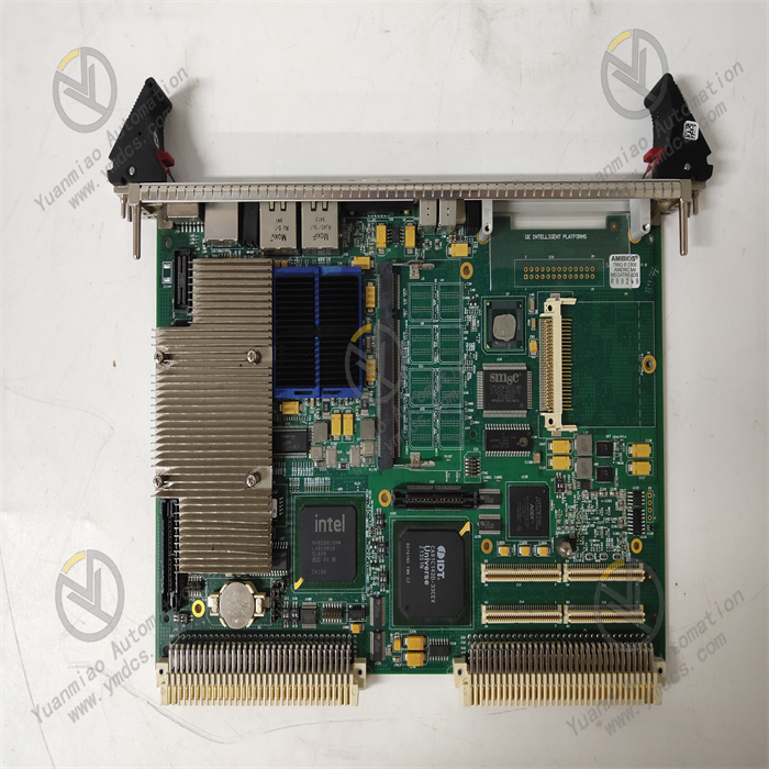
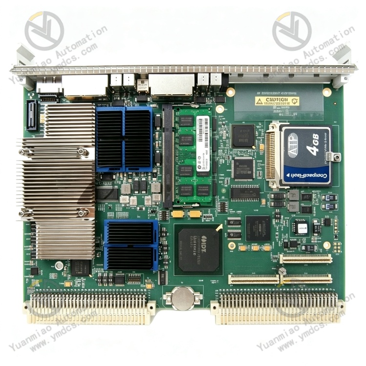
LAM 605‑109114‑003 is an original high‑precision RF impedance matching control board manufactured by Lam Research. It serves as a core process control component for semiconductor etch and thin‑film deposition equipment, specifically designed for the main control system of LAM 2300, Exelan and Flex series etchers. This board is mainly responsible for dynamic impedance matching of RF process loops, adaptive load adjustment, process signal acquisition and closed‑loop logic control. It is a critical component ensuring the stability, uniformity and repeatability of wafer etching and thin‑film deposition processes.
Integrating high‑precision signal acquisition, fast dynamic impedance adjustment, multi‑channel I/O linkage and real‑time process diagnosis, the board meets stringent requirements of semiconductor micro‑nano precision fabrication. It features fast response, superior matching accuracy, strong anti‑interference capability, consistent process performance and outstanding operational stability. Widely deployed in wafer manufacturing, semiconductor foundry and micro‑electronics precision processing, it fits engineering scenarios including OEM matching for new tools, board replacement for legacy semiconductor equipment, RF process system retrofitting and upgrade, and critical industrial spare‑parts inventory.
2. Functional Features
2.1 High‑Precision Dynamic RF Impedance Matching
The board realizes fully‑automatic dynamic impedance matching for RF process loops with a wide impedance adjustment range from 1 Ω to 2000 Ω. It adapts in real‑time to dynamic load impedance fluctuations during etching and deposition. The Voltage Standing Wave Ratio (VSWR) is stably controlled within 1.2:1, which greatly reduces RF signal reflection loss and ensures efficient and stable delivery of RF energy into process chambers. It eliminates process defects caused by impedance mismatch such as process drift, non‑uniform etching and thin‑film thickness deviation, so as to improve overall wafer yield.
2.2 Millisecond‑Level Ultra‑Fast Response Adjustment
Equipped with dedicated high‑speed control chips and adopting precision vacuum variable capacitor architecture, the impedance adjustment response time is less than 100 ms. It rapidly captures sudden load changes upon process startup, steady‑state operation and condition switching, and performs real‑time closed‑loop parameter correction. Zero adjustment lag and zero process oscillation are achieved, perfectly satisfying high‑frequency, high‑precision and continuous wafer production in semiconductor fabs.
2.3 Multi‑Signal Integrated Acquisition and Process Linkage
A 16‑bit high‑precision AD acquisition unit is embedded to collect and interpret analog I/O, digital I/O and chamber sensor signals. It synchronously links RF power supplies, gas flow control systems, vacuum modules and robot actuator systems for coordinated full‑process control of etching and deposition. It precisely matches tool main‑control logic to guarantee time‑sequence synchronization and high consistency of process parameters across multiple devices.
2.4 Comprehensive Process Self‑Diagnosis and Fault Protection
Hardware‑based multi‑dimensional self‑test logic enables real‑time monitoring and alarming for RF abnormality, impedance out‑of‑tolerance, loop failure, over‑temperature, communication error and load mismatch. Fault codes and process exception logs can be uploaded for root‑cause tracing and process review. Multi‑layer protection including over‑voltage, over‑current, over‑temperature and surge suppression prevents board burnout, process abortion and tool shutdown to sustain continuous stable equipment operation.
2.5 Dedicated Cooling Monitoring and Stable Thermal Control
Standardized cooling interfaces support both forced‑air cooling and De‑Ionized (DI) water cooling. Temperature and flow monitoring contacts are provided to track working temperature of the board and RF loops under heavy‑duty continuous‑process conditions. It avoids performance degradation and parameter drift induced by long‑time high‑power RF operation and guarantees long‑term process stability.
2.6 OEM‑Grade Compatibility with Excellent Process Adaptability
Custom‑developed for Lam Research etch and deposition tools, it natively fits main‑control architecture of mainstream platforms including 2300, Exelan and Flex. Power supply logic, communication protocols and process parameters are fully compatible for direct drop‑in replacement of legacy boards of the same part number. Its power architecture differs completely from the ‑004 revision to eliminate burn‑out risks from mis‑installation, suitable for OEM maintenance and retrofitting projects.
3. Technical Specifications
3.1 Basic Specifications
Part Number: 605‑109114‑003; Manufacturer: Lam Research; Product Type: RF Impedance Matching Control Board; Compatible Equipment: LAM 2300 / Exelan / Flex Series Etch & Thin‑Film Deposition Tools; Core Functions: Dynamic RF impedance matching, process closed‑loop control, multi‑signal acquisition & linkage, equipment fault diagnosis; Mounting: Standard plug‑in embedded installation inside control cabinet.
3.2 Impedance Matching Parameters
Impedance Adjustment Range: 1 Ω‑2000 Ω wide dynamic range; VSWR: Stably maintained below 1.2:1 with low reflection and low loss; Adjustment Response: <100 ms ultra‑fast dynamic response; Adjustment Mechanism: Coordinated control of precision vacuum variable capacitors and fixed capacitor banks to cover full‑range process load conditions.
3.3 Signal and Acquisition Parameters
Acquisition Accuracy: 16‑bit high‑resolution ADC with error‑free process parameter sampling; Signal Types: Analog AI/O, digital I/O and chamber sensor signals; Control Mode: Fully‑automatic closed‑loop adaptive regulation, supporting on‑line fine‑tuning and parameter memory; Linkage Capacity: Coordinated operation with RF power supply, gas system, vacuum unit and robot modules.
3.4 Electrical Specifications
Power Supply: Dedicated multi‑rail power (+5 V, +12 V, ±15 V), revision‑003‑specific (not interchangeable with ‑004); Circuit Design: Integrated regulation, filtering, surge suppression, over‑temperature and over‑current protection. Excellent RF noise immunity for high‑EMI environments inside semiconductor tools.
3.5 Environmental & Cooling Specifications
Operating Temperature: ‑20 ℃ ~ +60 ℃; Storage Temperature: ‑40 ℃ ~ +85 ℃; Cooling Options: Forced‑air cooling / DI‑water cooling, with integrated temperature and flow sensing contacts; Environmental Resistance: Dust‑proof, moisture‑proof, EMI‑resistant and high‑frequency‑RF‑interference‑resistant for clean‑room precision equipment; Operation Mode: 24‑hour non‑stop continuous process operation.
3.6 Physical Specifications
Dimensions: 100 mm × 80 mm × 35 mm; Weight: 0.25 kg; Construction: Industrial high‑grade PCB, high‑temperature and anti‑aging components, OEM precision SMT assembly for long‑term heavy‑duty precision semiconductor operation.
4. Hardware Configuration & Structural Advantages
4.1 Dedicated RF Hardware Architecture for Superior Process Accuracy
Adopting Lam‑custom RF control chips and vacuum variable capacitor assemblies optimized for high‑frequency RF etch/deposition processes. It delivers ultra‑high adjustment resolution with zero dead zone and responds sensitively to minor load variations. Hardware‑level guarantees are provided for uniformity and consistency of wafer processing to reduce process reject rate.
4.2 16‑Bit High‑Precision Acquisition for Accurate and Controllable Data
The 16‑bit high‑speed AD module implements isolated multi‑channel sampling to eliminate signal crosstalk and data drift. Tiny parameter variations throughout process cycles are captured, supplying reliable data for closed‑loop regulation, traceability and process optimization to satisfy micron‑level quality‑control requirements in semiconductor manufacturing.
4.3 Dual‑Mode Cooling with Thermal Monitoring for Long‑Term Stable Operation
Supporting both air and water cooling together with real‑time temperature and flow monitoring, the board adapts to high‑power long‑duration production. It mitigates performance degradation, parameter shift and hardware aging caused by overheating and extends service life significantly.
4.4 Dedicated Isolated Power Design to Prevent Mis‑installation Damage
Revision‑003 exclusive multi‑rail power architecture is electrically distinct from ‑004. Mechanical anti‑mismount features prevent board burn‑out and tool failure caused by wrong revision installation. Multi‑stage galvanic isolation provides strong immunity against in‑tool high‑frequency RF interference and enhances fault tolerance.
4.5 Compact Modular Design for Easy Maintenance
Light‑weight compact form factor fits original cabinet slots. Hot‑swap‑style plug‑in structure enables easy assembly‑disassembly with accurate positioning and reliable contact. Optimized PCB layout with anti‑aging traces facilitates inspection, process tuning, board replacement and calibration, effectively lowering maintenance costs.
5. Application Scenarios
- Semiconductor Etcher Process Control: RF impedance matching, closed‑loop regulation and wafer etch precision management for LAM 2300, Exelan and Flex series etchers.
- Core Regulation for Thin‑Film Deposition Tools: RF loop adaptation, load‑adaptive tuning and thin‑film thickness uniformity control for semiconductor PVD & CVD equipment.
- Precision Process Systems for Wafer Fabrication: Stable RF system control for foundry and micro‑electronics production lines to ensure batch‑to‑batch process consistency.
- Semiconductor Tool Retrofit & Upgrade: RF control module replacement, process accuracy enhancement and performance optimization for legacy LAM etch/deposition systems.
- OEM Maintenance & Spare‑Parts Support: Critical board inventory, emergency repair and routine replacement for compatible Lam Research production tools.
6. Product Advantages
- Superior process accuracy for higher production yield: Wide impedance tuning range, millisecond‑level response and tight VSWR control deliver stable RF energy delivery. Process fluctuation, etch non‑uniformity and thin‑film deviation are minimized to improve wafer processing precision and mass‑production yield.
- Strong anti‑interference performance and high fault tolerance: Dedicated galvanic isolation and multi‑layer protection against high‑frequency RF noise suit complex EMI environments inside semiconductor tools. Equipment failures induced by electrical anomalies, load variation and condition transitions are suppressed to guarantee 24‑hour fab uptime.
- Intelligent diagnosis for simplified maintenance and cost reduction: Multi‑dimensional self‑diagnosis and process traceability accelerate fault identification, shorten downtime and mitigate outage losses. It meets O&M requirements for modern smart semiconductor fabs.
- Long service life and favorable cost‑performance: Industrial‑grade hardware, dual‑mode thermal management and anti‑aging design realize low failure rate and long lifespan. Balancing process precision, stability and maintenance economy, it is a preferred critical spare‑part for semiconductor‑equipment maintenance and retrofitting.