I. Basic Information
Full Model:0190-11525
Brand & Origin:AMAT (Applied Materials, USA)
Product Positioning
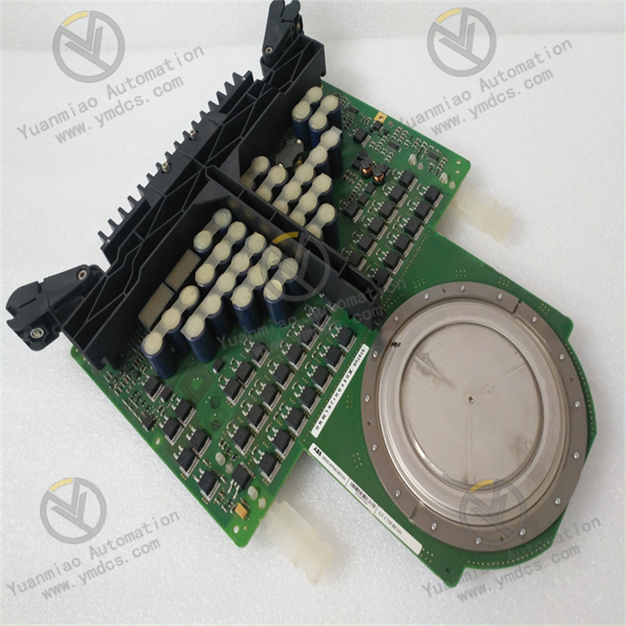
As an original special signal and power integrated cable assembly for AMAT semiconductor wafer processing equipment, it is a core supporting accessory for high-end semiconductor process equipment such as etchers, thin film deposition systems, ion implanters and diffusion furnaces. Designed exclusively for cleanroom and high-precision process conditions of semiconductor workshops, it is mainly used for signal transmission, power supply and data interaction between equipment main control units, drive modules, sensors, actuators and the overall control system. As the core carrier of equipment hardware links, it ensures distortion-free transmission of precision process signals and uninterrupted stable power supply, eliminating process deviation, equipment alarm, process interruption and wafer defects caused by line interference, poor contact and line aging. Exclusively compatible with corresponding original AMAT process equipment, it serves as a special supporting part for original equipment assembly, fault replacement, equipment maintenance, overall refurbishment and production line expansion, and is a key consumable accessory to ensure the stability and yield of semiconductor precision processes.
Hardware Architecture
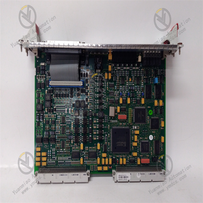
It adopts an integrated wiring architecture dedicated to semiconductor equipment, integrating multi-core shielded signal wires, insulated power wires, high-temperature resistant filling layers, full-domain shielding layers and wear-resistant protective outer jackets. The wire core is made of high-purity oxygen-free copper conductor with excellent conductivity and extremely low impedance, which can accurately transmit weak precision process signals and stable power supply. Internal signal wires are independently shielded and arranged in partitions to completely eliminate inter-wire crosstalk and signal coupling interference. Adopting a multi-layer insulation protection design, the inner layer is a high-density flame-retardant insulation layer, the middle layer is a full-domain copper braided shielding layer, and the outer layer is a special jacket resistant to high and low temperature, chemical corrosion and wear. Pre-installed with original standard connectors and terminals, it features precise crimping process, stable contact resistance and reliable locking, with no risk of virtual connection, loosening or oxidation, fully adapting to the harsh working conditions of high-frequency start-stop, continuous operation and precision process regulation of semiconductor equipment.
Mounting Specification
It strictly follows the original AMAT equipment wiring standards, with wire harness length, connector model, pin definition, wiring radian and fixing points fully matching the original equipment structure. It supports fixed internal equipment wiring and snap-on positioning installation, adapts to compact cabinet layout and reciprocating displacement working conditions of mechanical moving parts, and is resistant to bending damage and loosening and disconnection under long-term equipment vibration and alternating temperature changes. The original precise matching interface features smooth plugging and firm locking, requiring no modification, adapter or re-crimping during installation, enabling direct in-situ replacement of old and damaged wire harnesses, and adapting to rapid maintenance and non-stop overhaul operations, fully complying with the installation and operation specifications of semiconductor cleanroom equipment.
Compatible Systems
Natively compatible with the full range of AMAT semiconductor processing equipment, including core wafer process equipment such as etching, PVD/CVD deposition, ion implantation and heat treatment diffusion equipment. It perfectly matches the signal protocol, power supply parameters and interface definition of the original equipment main control system, drive control system, sensor monitoring system and actuator power system, enabling seamless connection with various functional modules of the equipment without parameter debugging or hardware adaptation, and can work normally after installation. Exclusively adapted to the original equipment program logic and hardware link architecture without compatibility conflicts, it is the only compliant supporting wire harness for original equipment maintenance, fault replacement and overall refurbishment.
Product Characteristics
As an original precision process dedicated wire harness of AMAT, it has passed strict full-item tests including continuity test, impedance detection, signal integrity test, insulation voltage resistance test, high and low temperature aging and bending resistance test, as well as dust-free cleaning treatment before delivery. It features zero-distortion signal transmission, stable power supply without fluctuation, strong electromagnetic interference resistance, high and low temperature resistance, chemical corrosion resistance, wear and bending resistance and long-term anti-aging performance. With excellent shielding performance, it can effectively isolate strong electromagnetic interference generated by high-frequency drive modules, radio frequency modules and power components inside semiconductor equipment, ensuring accurate transmission of precision process signals. The overall dust-free, oil-free and non-precipitation design meets the high cleanroom standards of semiconductor workshops, avoiding wafer process environmental pollution caused by line dust. It maintains stable operating parameters without performance attenuation or line faults for a long time, greatly reducing equipment alarm shutdown and process defect probability.
II. Technical Specifications
1. Harness Structure & Material Parameters
Conductor Material: Made of high-purity oxygen-free copper core with high conductivity, uniform resistance and extremely low signal loss, adapting to synchronous transmission of weak analog signals, high-frequency digital signals and low-voltage power supply. Insulation Material: Imported special flame-retardant insulation material with excellent insulation performance and high voltage resistance, resistant to high temperature, aging and electric leakage, eliminating risks of inter-wire short circuit, electric leakage and insulation breakdown. Shielding Structure: Full-area covered copper mesh shielding layer combined with independent single-core shielding design forms a dual anti-interference architecture, which can comprehensively isolate external electromagnetic radiation, inter-wire crosstalk and ground loop interference to ensure signal integrity. Outer Jacket Material: Special jacket resistant to high and low temperature, acid and alkali corrosion, organic solvent and high wear, adapting to special process environments of semiconductor equipment, resistant to erosion of process gas and trace chemical fog, not easy to crack, age or damage.
2. Electrical Performance Parameters
Conduction Performance: High consistency of overall harness conduction with stable contact resistance, no breakpoint, no virtual connection and no resistance drift, ensuring lossless signal transmission and no voltage drop in power supply. Insulation Voltage Resistance: High insulation and voltage resistance performance, capable of withstanding conventional electrical pressure difference of equipment, eliminating insulation breakdown, electric leakage and cross-current faults, adapting to mixed high and low voltage wiring conditions of equipment. Signal Transmission Characteristics: Stable high-frequency signal transmission with accurate time sequence, no waveform distortion and no data packet loss, meeting the millisecond-level control and high-precision parameter regulation signal transmission requirements of semiconductor precision processes. Anti-Interference Index: Excellent electromagnetic shielding efficiency, effectively resisting radio frequency interference, frequency conversion interference and power cable electromagnetic coupling interference inside equipment, ensuring accurate process control signals and monitoring data.
3. Mechanical Performance Parameters
Bending Resistance: Passed ten-thousand-level standard bending test, with wire core not easy to break and jacket not easy to crack, adapting to reciprocating bending and dynamic wiring working conditions of equipment moving parts. Tensile and Compressive Resistance: Compact harness structure with good tensile, compressive and torsion resistance, not easy to deform or damage during equipment installation, fixing and daily operation and maintenance. Connector Connection Performance: Precisely crimped original terminals with moderate plugging and locking force, stable connection and anti-loosening and anti-disengagement functions, no loosening or poor contact under long-term vibration conditions, eliminating intermittent line faults.
4. Environmental Resistance Parameters
Temperature Resistance: Adapted to the operating temperature range of semiconductor equipment, capable of long-term resistance to local high temperature inside equipment and conventional temperature difference changes in workshops, no hardening and cracking at low temperature, no softening and deformation at high temperature. Corrosion Resistance: Resistant to erosion of trace acid-base gas and organic solvent fog in semiconductor processes, no aging, pulverization or cracking of the jacket, adapting to special corrosion working conditions of process equipment. Cleanliness Performance: Dust-free, non-precipitation, oil-free and particle-free, complying with Class100/Class1000 semiconductor cleanroom cleanliness standards, unable to pollute wafers, process cavities and process environments.
5. Working Condition Adaptation Parameters
Operating Temperature:-10℃~+70℃
Storage Temperature:-20℃~+80℃
Operating Humidity:10%~90% RH, non-condensing
III. Key Features
1. High-Fidelity Signal Transmission & Precision Process Guarantee
Adopting independent split-core shielding and full-domain electromagnetic shielding architecture, it completely solves the problems of signal crosstalk, waveform distortion and data drift under high-frequency working conditions of semiconductor equipment. It can accurately transmit equipment process control signals, cavity monitoring signals, position feedback signals and temperature and pressure sampling signals, ensuring precise and controllable core process parameters such as equipment etching rate, film thickness and ion implantation dosage. It eliminates wafer process deviation, parameter error and product defects caused by line signal distortion, and guarantees the stability and high yield of semiconductor precision processes from the hardware link level.
2. Stable Power Supply & Elimination of Equipment Abnormal Shutdown
The wire harness conductor features low impedance, stable conduction and no intermittent breakpoints, which can provide continuous and stable power supply and working voltage for equipment drive modules, sensing units and actuators, eliminating line voltage drop, power supply fluctuation and instantaneous power failure. It effectively avoids equipment error reporting, process interruption, cavity reset and overall shutdown faults caused by poor line contact and unstable power supply, ensuring continuous and uninterrupted production of semiconductor production lines and reducing unplanned shutdown losses.
3. High Weather Resistance & Adaptation to Harsh Process Conditions
Made of special corrosion-resistant, high-temperature resistant, wear-resistant and clean materials, it is specially adapted to the special working conditions of semiconductor equipment such as high-temperature operation, trace chemical corrosion, high-frequency electromagnetic interference and dust-free cleanliness. Different from ordinary industrial wire harnesses, it can resist long-term erosion of process gas, organic solvent and sharp temperature changes, without jacket aging, wire core oxidation, insulation failure and dust precipitation, perfectly matching the stringent production requirements of high precision, high cleanliness and high stability of wafer manufacturing, and adapting to long-term continuous operation of equipment.
4. Original Precise Adaptation & Non-Destructive Quick Replacement
The interface model, pin definition, wire harness length and wiring specifications are 100% matched with original AMAT equipment, requiring no wire cutting, re-crimping or debugging adaptation, enabling direct in-situ replacement of old and faulty wire harnesses with aging damage, electric leakage, abnormal signals and poor contact. It adapts to rapid equipment maintenance operations, greatly shortening equipment shutdown maintenance time and improving production line operation and maintenance efficiency, fully meeting the low shutdown and high productivity production requirements of semiconductor production lines.
5. Dust-Free Clean Design for High-End Cleanroom Adaptation
The overall wire harness is treated with dust-free cleaning and vacuum packaging, with no dust, particle precipitation or oil residue on the material, strictly complying with semiconductor cleanroom cleanliness standards. It will not cause dust pollution to wafers, process cavities and core precision equipment components, eliminating process defects and precision component jamming and wear caused by impurities, adapting to the high-cleanliness production environment of high-end wafer and chip precision manufacturing.
IV. Working Principle
As a special connecting wire harness component for semiconductor process equipment, AMAT 0190-11525 serves as the core physical link for signal transmission and power delivery between various functional modules of the equipment, realizing interconnection and intercommunication of the equipment control system, power system, sensing system and actuator system. After the equipment is powered on normally, the entire wire harness component maintains stable conduction, reliable insulation and effective shielding throughout the operation, providing basic hardware link support for equipment operation.
In terms of power transmission, the wire harness power core stably transmits the total equipment power supply to each drive module, actuator and sensing unit, ensuring stable and fluctuation-free voltage and current throughout the process, and avoiding abnormal module operation and equipment start-stop faults caused by abnormal power supply. In terms of signal transmission, the independently shielded signal wires transmit equipment process control instructions, cavity condition monitoring data, position feedback signals and temperature and pressure parameters in real time. The full-domain shielding structure isolates external electromagnetic interference, ensuring accurate time sequence, complete waveform and error-free data of signal transmission, and supporting the equipment to complete precise process actions such as etching, thin film deposition and ion implantation.
Throughout the equipment operation process, the wire harness resists the impact of internal high temperature, vibration, electromagnetic interference, trace chemical corrosion and other working conditions by virtue of excellent insulation, wear resistance, corrosion resistance and aging resistance, eliminating link faults such as line short circuit, electric leakage, signal distortion and poor contact. The stable hardware link ensures constant equipment process parameters, normal operation logic and accurate condition monitoring, and continuously supports the stable and efficient operation of semiconductor precision processes.
V. Application Scenarios
1. Original AMAT Semiconductor Equipment Matching: Exclusively applicable to full-series wafer process equipment of Applied Materials, including etchers, PVD/CVD thin film deposition equipment, ion implanters and heat treatment diffusion equipment, used as the original standard connecting wire harness for equipment assembly.
2. Fault Wire Harness Replacement and Equipment Maintenance: Used to replace old wire harnesses with aging cracking, line electric leakage, abnormal signals and poor contact, solving equipment faults such as frequent alarms, unstable processes and intermittent shutdowns, and restoring the original operating state of equipment.
3. Overall Refurbishment and Upgrade of Semiconductor Equipment: Adapted to second-hand equipment refurbishment, equipment disassembly and recombination, and production line equipment transformation scenarios, replacing aging and invalid wire harnesses to improve the overall stability and process accuracy of equipment and ensure qualified production after refurbishment.
4. High-Cleanliness Precision Process Scenarios: Applied to high-precision manufacturing production lines of high-end wafers, chips and semiconductor devices, meeting the stringent requirements of high-precision processes for equipment link stability and production environment cleanliness by virtue of dust-free, high anti-interference and high stability characteristics.