Description
Product Overview
Model No.:678-087532-001 (Original LAM Part)
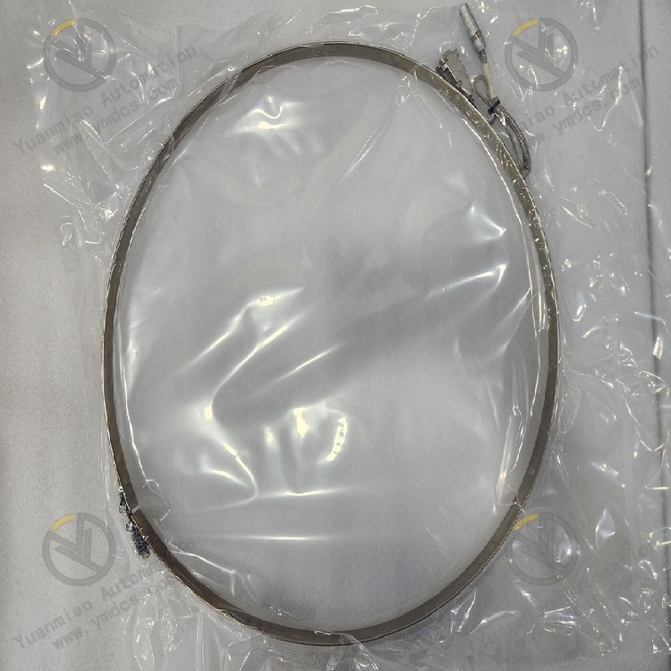
This is a factory-calibrated core precision optical laser inspection component manufactured by LAM Research. It serves as a high-precision optical measuring part specially designed for semiconductor etchers and thin-film deposition equipment. Its hardware structure, optical parameters and mounting dimensions are fully fixed with no universal interchangeable alternatives. Spare parts of the same part number support direct on-site replacement without optical path recalibration, equipment program modification or mechanical assembly alteration. It is a critical spare part for routine maintenance and component replacement in wafer fabrication equipment.Brand:LAM
System Compatibility
Exclusively applicable to LAM series etchers, PVD/CVD thin-film deposition equipment and wafer process inspection tools. Its main functions include wafer position correction, chamber alignment, laser distance measurement, optical signal feedback and precision positioning & control of equipment. As the core of the equipment’s optical closed-loop inspection system, it guarantees wafer machining accuracy, chamber tightness and alignment consistency. LAM strictly controls production batches for this part with long-term supply available and no EOL (End of Life) discontinuation plan.
Core Product Definition
A high-precision laser optical measurement component dedicated to semiconductor equipment, integrating a precision lens assembly, optical filtering circuit, laser focusing unit and position feedback sensor. It emits and receives high-precision laser beams to perform real-time detection of wafer position, acquisition of chamber alignment deviation and feedback of mechanical movement travel. Optical signals are converted into accurate positional data recognizable by the equipment, providing a high-precision optical reference for sophisticated semiconductor manufacturing processes and equipment closed-loop servo control. It acts as a core precision sensing unit for advanced wafer fabrication tools.
Six Core Hardware Functional Modules
1. High-Precision Laser Focusing Optical Unit
Equipped with a custom factory precision lens group and coated optical lenses, delivering outstanding optical focusing accuracy and uniform laser spots to output stable collimated laser beams. The lenses adopt multi-layer anti-reflection and anti-interference coating technology to effectively filter stray light and ambient refraction interference. The optical path maintains zero offset and focal length drift during long-term operation, meeting the micron-level precision positioning requirements for semiconductor inspection.
2. Real-Time Position Sensing & Feedback Unit
Built with a high-sensitivity photoelectric receiving and signal conversion structure that rapidly captures variations in reflected laser signals to accurately identify wafer offset, chamber alignment error and mechanical travel deviation. Standard feedback signals are output in real time to form a closed-loop detection workflow: Laser Emission → Reflection Acquisition → Data Feedback, supplying real-time data for equipment servo adjustment, position correction and deviation compensation.
3. Optical Noise Filtering & Purification Unit
Integrates a physical optical filtering structure to block stray light originating from internal equipment light refraction, dust diffuse reflection, ambient illumination and residual light inside process chambers. It eliminates false detection, data jitter and positioning deviation caused by stray light, ensuring stable and accurate optical inspection within complex chamber environments.
4. Precision Mechanical Positioning & Mounting Unit
Adopts an integrated precision die-cast structure with ultra-tight assembly tolerances and high-precision mounting datum planes to guarantee consistent positioning after each reinstallation. The rigid structure resists equipment vibration and thermal deformation, preventing optical path displacement induced by tiny mechanical shifts, and adapts to high-frequency precision motion and 24/7 continuous operation of semiconductor equipment.
5. Wide-Temperature Stable Anti-Aging Optical Unit
All optical components and structural parts are fabricated from semiconductor-grade highly stable materials with an ultra-low thermal expansion coefficient, capable of withstanding transient thermal shocks and temperature fluctuations inside process chambers. The lenses feature anti-aging, anti-fogging and anti-coating-peeling properties, with no optical path attenuation or precision degradation over extended runtime, supporting non-stop high-precision process execution for semiconductor tools 24 hours a day, 7 days a week.
6. Dust-Proof Sealed Protection Unit
Features a hermetically sealed integrated housing that prevents dust, oil stains and microparticles from entering the optical cavity, compliant with cleanroom standards for semiconductor manufacturing. It avoids optical path obstruction, inspection failure and accuracy decline caused by wafer debris and tiny particles from process exhaust, greatly reducing cleaning frequency and maintenance costs for the optical assembly.
Technical Specifications
(1) Basic Hardware Specifications
| Item | Technical Parameter |
|---|---|
| Full Part Number | 678-087532-001 |
| Equipment Type | Precision Laser Optical Measurement Component for LAM Semiconductor Equipment |
| Compatible Equipment | LAM Etchers, Thin-Film Deposition Tools, Wafer Process Alignment Equipment |
| Core Functions | Laser Ranging, Wafer Alignment, Chamber Positioning, Position Deviation Feedback |
| Optical Accuracy | Micron-level precision detection with stable optical path free of drift |
| Structural Feature | Integrated dust-tight sealed structure with precision mounting datum surfaces |
| Applicable Working Condition | Semiconductor cleanroom environment with continuous process operation |
| Protection Class | Highly sealed against dust and oil (embedded dedicated for equipment internal use) |
(2) Optical & Operating Core Parameters
- Laser Optical Path Characteristic: Collimated focusing optical path with highly uniform laser spot; no offset or divergence during long-term operation
- Detection Accuracy: Micron-level positioning feedback precision to meet alignment demands of sophisticated semiconductor processes
- Anti-Interference Performance: Multi-layer optical coating plus physical filtering to block stray light, diffuse reflection and ambient light interference
- Structural Stability: Low-expansion precision structure with vibration and thermal deformation resistance; extremely high repeat mounting accuracy
- Anti-Aging Performance: Lenses resist fogging, coating peeling and signal attenuation with stable precision over long service life
- Feedback Performance: High-speed optical signal acquisition with fast response to support dynamic servo correction of equipment
(3) Environmental & Compliance Specifications
- Operating Temperature: 18℃ ~ 28℃, constant temperature standard for semiconductor cleanrooms
- Thermal Shock Resistance: Tolerates short-term process thermal shocks and temperature fluctuations inside equipment chambers
- Operating Humidity: 40% ~ 60%RH, no condensation or oil adhesion allowed
- Cleanroom Compatibility: Compliant with Class 100 / Class 10 semiconductor clean manufacturing environments
- Mechanical Vibration Resistance: Tolerates high-frequency micro-vibration of equipment without optical path shift or structural loosening
- Operation Mode: Supports 24/7 non-stop high-precision inspection operation
Product Advantages
Ultra-High Micron-Level Optical Inspection PrecisionCustom factory coated lens assembly delivers precise optical focusing and exceptional long-term stability, eliminating focal length drift and laser spot divergence, and ensuring micron-level process precision for wafer alignment and chamber positioning in semiconductor production.
Strong Anti-Interference Optical Path Design
Multi-layer optical filtering and anti-stray-light architecture effectively suppress internal equipment diffuse reflection, dust refraction and ambient light interference, eliminating detection data fluctuation and positioning deviation, and adapting to complex working conditions inside process chambers.Integrated High-Stability Mechanical Structure
Precision die-cast low-thermal-expansion structure with high-precision mounting datum features excellent anti-vibration and anti-thermal-deformation capability. Repetitive installation maintains consistent positioning with no need for repeated optical path calibration, significantly cutting commissioning workload.Long Service Life & Low Maintenance Requirements
Semiconductor-grade optical materials prevent lens fogging, coating peeling and optical attenuation. Component precision barely degrades during long-term equipment operation, extending maintenance cycles and reducing spare part replacement frequency.Closed-Loop High-Precision Feedback Control
High-speed optical signal acquisition and positional feedback compensate in real time for mechanical deviation and thermal deformation error of equipment, guaranteeing continuity and consistency of equipment servo regulation and wafer fabrication processes, and improving production yield stability.Direct On-Site Replacement with Minimal Downtime
Standard factory mounting dimensions and interfaces allow direct replacement of faulty units with no equipment program modification, mechanical adjustment or complex optical path calibration required, maximizing maintenance efficiency and minimizing production downtime.Application Scenarios
1. Precision Alignment System for LAM Etching Equipment
Used for alignment inspection during wafer loading, chamber closure and etching station positioning. It feeds back positional deviation in real time to assist the equipment in micron-level precise positioning, ensuring uniform etching and accurate pattern definition on wafers, and avoiding process defects caused by misalignment.
2. Optical Inspection System for Thin-Film Deposition Equipment
Compatible with PVD and CVD thin-film deposition tools, applied to chamber sealing alignment, wafer station correction and mechanical travel limit detection. Stable optical feedback guarantees uniform thin-film thickness and repeatable process results, supporting stable production of advanced thin-film processes.
3. Wafer Transfer & Positioning System for Semiconductor Tools
Deployed in wafer robot handling, station switching and wafer chuck alignment inspection. It rapidly and accurately identifies wafer positional status to prevent offset, wafer jamming and alignment anomalies, ensuring collision-free, deviation-free and stable wafer transfer workflows.
4. Chamber Condition Monitoring System for Equipment
Detects chamber closing precision, sealing positional deviation and mechanical structural deformation via laser optical paths, feeds back abnormal chamber status in real time, and provides early warning of structural offset and assembly loosening risks to secure process stability and operational safety of production equipment.
5. Technical Upgrade & Maintenance for Legacy LAM Equipment
Replaces aging optical assemblies suffering from optical attenuation, lens fogging, degraded positioning accuracy and frequent alignment alarms. On-site direct replacement restores equipment process precision without equipment structural or program modification, boosting equipment uptime and production yield.