Description
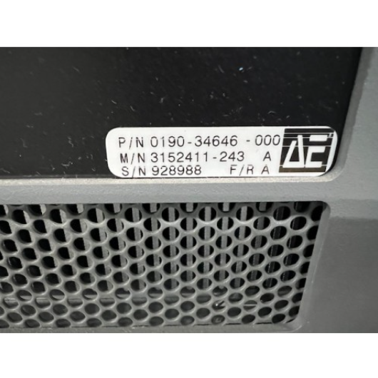
AMAT 0190-34646
I. Basic Information
Part Number: 0190-34646
Brand: Applied Materials (AMAT)
Product Type: High-frequency low-loss RF coaxial cable assembly, specially designed for high-precision RF signal transmission of semiconductor wafer etching and thin-film deposition equipment. It serves as a core RF connecting spare part for plasma process equipment to ensure low-loss and high-stability signal transmission.
Compatible Platform: Applicable to AMAT series etchers, PVD/CVD deposition equipment and plasma process tools, matching RF excitation and high-frequency bias signal transmission scenarios.
Product Positioning
AMAT 0190-34646 is an OEM dedicated RF coaxial cable assembly for high-end semiconductor process equipment. Adopting low VSWR, low attenuation and high-shielding materials with precision integrated connectors, it achieves full-link impedance matching. It stably transmits RF power and high-frequency bias signals for process chambers, suppresses signal reflection, harmonic loss and external electromagnetic interference, and ensures plasma ignition stability and wafer processing uniformity. With high temperature resistance, aging resistance and vibration resistance structure, it adapts to harsh on-site working conditions and effectively avoids process drift and equipment failure caused by signal mismatch.
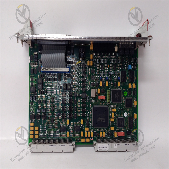
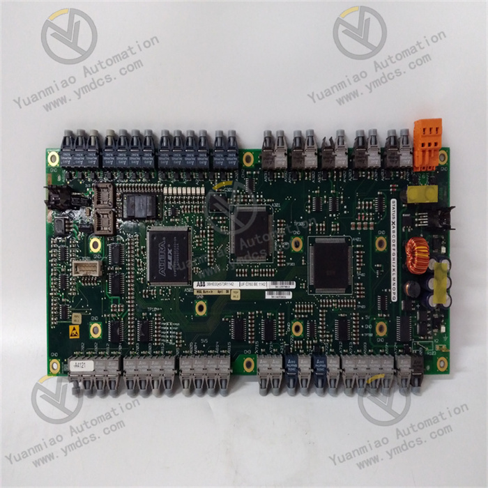
Hardware Structure
The cable assembly consists of four core parts: low-loss coaxial cable body, precision RF connectors, stress buffer reinforcement structure and anti-corrosion outer sheath, featuring integrated impedance matching and no signal breakpoint loss.
1. Low-Loss RF Coaxial Cable Body
Adopting silver-plated oxygen-free copper inner conductor and low-dielectric foamed insulation material to reduce high-frequency skin effect loss. Double-layer copper braided shield + aluminum foil fully shields electromagnetic interference, ensuring high signal purity in complex electromagnetic environments.
2. OEM Precision RF Connector Unit
Integral crimping molding with low contact resistance and polished end face realizes reflection-free high-frequency signal docking, fully matching original equipment interface standards without adapter accessories.
3. Stress Buffer Reinforcement Unit
Flexible buffer sheath at the connector root resists bending fatigue and vibration impact, preventing core wire breakage and shield damage caused by long-term equipment operation and maintenance disassembly.
4. High-Temperature Anti-Corrosion Outer Sheath
Flame-retardant, oil-proof and corrosion-resistant special sheath adapts to long-term high-temperature radiation and chemical cleaning environment of process equipment, delaying cable aging and cracking.
Installation Specifications
- Installation Method: Point-to-point fixed embedded installation for RF link connection of process equipment, supporting in-situ replacement and maintenance
- Impedance Standard: 50Ω full-link precise impedance matching
- Connector Type: AMAT OEM dedicated RF connector
- Tool Matching: RF torque wrench, anti-static wristband, fixing clips
Product Features
1. Ultra-Low High-Frequency Signal Loss
Minimizes RF power attenuation and signal distortion, stabilizes plasma energy, and ensures consistent wafer processing parameters in mass production.
2. Full-Band High Shielding Performance
Double-layer 360° shielding isolates external electromagnetic crosstalk, effectively avoiding plasma jitter, chamber arcing and process abnormal defects.
3. Precise 50Ω Impedance Matching
Controls VSWR within the standard range, suppresses signal reflection, and protects core equipment such as RF power supplies and matching networks from reflected power impact.
4. Industrial-Grade Durability
Excellent bending resistance, high temperature resistance and aging resistance adapt to 7×24-hour uninterrupted mass production operation, reducing maintenance frequency and equipment downtime.
5. OEM Integrated Molding & Compatibility
Original integrated crimping design with perfect compatibility with AMAT equipment, supporting direct in-situ replacement without wiring modification.
II. Technical Specifications
2.1 RF Transmission Parameters
- Characteristic Impedance: 50Ω ±1Ω
- Frequency Range: Compatible with semiconductor process RF frequency band
- Voltage Standing Wave Ratio (VSWR): ≤1.2
- Shielding Effectiveness: Full-band high anti-interference level
- Transmission Attenuation: Ultra-low high-frequency attenuation for process precision requirements
2.2 Electrical Safety Parameters
- Withstand Voltage: Meet equipment RF high-voltage insulation standards
- Insulation Resistance: Ultra-high insulation, no signal leakage
- Contact Resistance: Ultra-low contact resistance without heating and attenuation abnormality
2.3 Environmental Specifications
- Operating Temperature: -20℃ ~ +85℃
- Storage Temperature: -40℃ ~ +90℃
- Operating Humidity: 10%~90% RH (non-condensing)
- Durability: Oil-proof, corrosion-resistant, flame-retardant, vibration-resistant and bending-resistant
III. Key Features
1. High-Precision Low-Loss RF Transmission
Stably transmits RF excitation and bias signals, maintains stable plasma state, and guarantees consistency of wafer etching and deposition processes.
2. Full-Link Impedance Matching & Equipment Protection
Suppresses signal reflection, avoids impact of reflected power on core RF equipment, and reduces hardware failure rate and maintenance cost.
3. Strong Anti-Interference & Process Stability
Eliminates electromagnetic crosstalk noise, prevents process jump, chamber arcing and wafer defects, and improves production yield.
4. High Durability for Uninterrupted Mass Production
Industrial reinforced structure adapts to harsh working conditions, reduces cable aging failure and equipment downtime.
IV. Working Principle
As a dedicated transmission link for semiconductor equipment RF systems, AMAT 0190-34646 connects RF power supplies, matching networks and process chambers. The high-frequency RF power and bias signals output by the RF power supply are completely transmitted to the chamber electrode through the cable, exciting internal gas to generate stable plasma for wafer processing.
The precise 50Ω impedance matching eliminates signal reflection and attenuation, and the double-layer shielding structure isolates external electromagnetic interference. The stress buffer structure absorbs vibration and bending stress, ensuring long-term stable signal transmission and consistent process parameters.
V. Application Scenarios
1. Semiconductor dry etching process equipment RF signal transmission
2. PVD/CVD thin-film deposition equipment RF link connection
3. Plasma cleaning and surface modification process equipment
4. OEM cable replacement and maintenance for AMAT process equipment