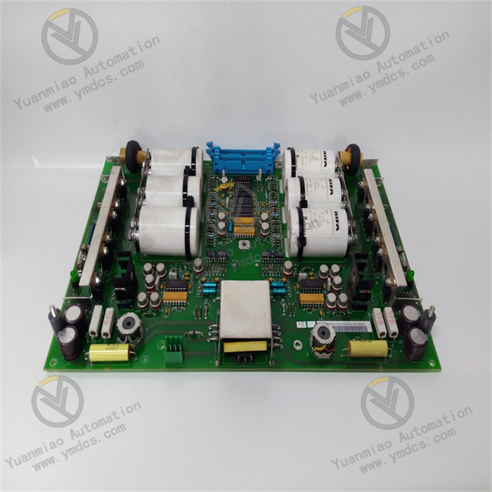
Description
1. Product Overview
Model: 853-043759-006
Brand: LAM RESEARCH
Product Name: Signal Acquisition & Control Board / Process Conditioning Interface Board for Semiconductor Etch Equipment
Product Positioning
853-043759-006 is a core board component originally supplied by LAM RESEARCH for high-end semiconductor etch equipment. Developed specifically for precision processes of wafer dry etching and plasma etching, it serves as a critical hardware unit responsible for equipment process signal acquisition, signal conditioning, logic interaction, closed-loop control and safety interlock. Acting as the core signal transfer and control hub between the equipment main control system, process chambers, plasma modules, sensor detection units and actuator drive assemblies, it performs key functions including precise sampling of process signals, noise filtering, signal shaping, command parsing, status feedback and fault protection. It is an essential original maintenance spare part that guarantees nanometer-scale process accuracy, process consistency and long-term stable availability of LAM etch tools.
Core Functions
It collects real-time core process data such as plasma parameters inside etch chambers, chamber pressure, process temperature, gas flow rate and RF matching status. High-precision filtering, amplification, calibration and signal shaping are implemented on weak, high-frequency and interference-prone raw process signals to eliminate high-frequency clutter caused by plasma discharge and RF operation. It accurately receives and parses process recipe commands issued by the equipment main controller, executes signal logic operation and closed-loop feedback regulation to dynamically satisfy variable parameter requirements of etching processes. Embedded hardware-based safety interlock and anomaly monitoring mechanisms continuously monitor chamber conditions, signal links and equipment operating status. Protection latching will be triggered rapidly upon parameter overrange, signal abnormality or chamber failure to avoid etching offset, non-uniform wafer etching, chamber anomalies and equipment shutdown due to alarms. It fully ensures stability, repeatability and high precision of semiconductor dry etching processes, supports 7×24-hour non-stop mass production on wafer fabrication lines, and effectively improves wafer yield and overall equipment efficiency.
Applicable Systems
Exclusively compatible with all mainstream dry etch equipment platforms of LAM RESEARCH, supporting 200mm/300mm wafer etching tools and matching the main control architecture of production plasma etchers, dielectric etchers and metal etchers. Fully compliant with original equipment protocol and hardware interface standards. It supports replacement of legacy boards, equipment maintenance, production line capacity expansion and equipment upgrade, featuring excellent versatility and interchangeability between new and existing equipment with zero compatibility risks.
Application Scenarios
Widely deployed in 200mm / 300mm semiconductor wafer fabrication lines, covering precision dry plasma etching processes for chip logic devices, memory devices, power semiconductors and advanced wafer packaging. Adopting dedicated card-mount installation structure inside equipment cabinets, it is designed for high-precision, high-stability and zero-tolerance production conditions in semiconductor cleanrooms. It is a critical spare part for routine maintenance, fault replacement and equipment servicing of LAM etch systems.
2. Technical Features
Precise Processing of High-Frequency Process Signals for Complex Plasma Etching Conditions
Equipped with high-spec signal processing IC dedicated to semiconductor etch equipment with optimized algorithms targeting high-frequency signals, weak sensor signals and dynamically fluctuating process signals in plasma etching environments. It supports multi-stage high-frequency digital filtering, electromagnetic noise suppression, linear error calibration and dynamic temperature drift compensation. Minor process variations including subtle chamber pressure changes, plasma power fluctuations, gas flow deviations and chamber temperature drift can be captured accurately. Benefiting from high signal acquisition resolution, favorable linearity and outstanding repeatability, it fully meets stringent process control standards for nanometer-scale wafer etching and eliminates etching defects and yield loss induced by process parameter drift at the hardware level.
Proprietary Original Process Logic Delivering High Closed-Loop Control Accuracy
Embedded with LAM RESEARCH proprietary etch process control logic and closed-loop operation algorithms, deeply adapted to dynamic characteristics of dry plasma etching. It enables real-time comparison of etching parameters, dynamic deviation correction and process status tracking control. Capable of adapting to full-cycle operating conditions including chamber ignition, plasma stabilization, continuous etching and process termination, it dynamically balances various process parameters to guarantee intra-wafer etching uniformity and batch-to-batch process consistency, effectively resolving process issues such as uneven etch rate, profile deviation and poor process repeatability.
Integrated Multi-Channel Signal Processing with Broad Equipment Adaptability
The board integrates multiple dedicated analog and digital process signal channels for simultaneous parallel acquisition, processing and output of various process signals including pressure, temperature, flow rate, RF status, switch interlock and chamber status, realizing integrated management of multi-dimensional process parameters. It combines signal conditioning, operation conversion, command driving, data communication and interlock protection without external adapter modules, simplifying the internal control architecture of equipment and satisfying multi-scenario process signal management demands of all LAM etch tools.
Industrial-Grade Anti-Interference Design for Harsh Process Environments
Constructed with premium industrial-grade original components, precision PCB impedance-controlled routing and gold-plated anti-corrosion contacts, tailored to operating conditions of etch equipment featuring intense RF interference, plasma electromagnetic radiation, alternating temperature variation and strict cleanroom requirements. Built-in opto-electrical isolation, surge suppression, EMC shielding, electrostatic protection and overcurrent/overvoltage protection circuits effectively resist RF harmonics, electrostatic pulses, electromagnetic crosstalk and ambient temperature variation. With dust-proof, moisture-proof and anti-aging properties, it maintains stable operation under long-duration heavy load without signal distortion or parameter drift, delivering extremely high operational reliability
Intelligent On-Board Self-Diagnosis Enabling Efficient Maintenance & Troubleshooting
Equipped with on-board intelligent self-diagnosis monitoring system that continuously tracks hardware chip status of the board, operating conditions of each signal channel, bus communication links, power supply and abnormal process parameters. It accurately locates channel failures, signal disconnection, data anomalies, communication breakdown, hardware damage and parameter disorder. Original equipment fault codes and operation logs are generated automatically, supporting online access via equipment host for fault tracing and operation review. It greatly shortens downtime for troubleshooting, maintenance and commissioning and reduces production line maintenance costs and outage losses.
Standardized Original Design with Superior Interchangeability & Versatility
Strictly developed in accordance with LAM RESEARCH original hardware specifications, interface definitions, communication protocols and mounting standards, adopting standardized modular card structure dedicated to equipment. Board dimensions, mounting positions, interface pins, communication protocols and electrical parameters are fully compatible with original equipment. Aged or faulty boards can be directly hot-swapped in situ without modifying equipment programs, adjusting wiring or reconfiguring parameters. It is applicable to full scenarios including equipment maintenance, capacity expansion, production line renovation and equipment upgrade with zero compatibility risks.
3. Specification Parameters
| Item | Parameter |
|---|---|
| Model | 853-043759-006 |
| Manufacturer | LAM RESEARCH (USA) |
| Equipment Type | Process Signal Acquisition & Control Board, Process Conditioning Interface Board for Semiconductor Etch Equipment |
| Compatible Equipment | All dry plasma etch systems of LAM RESEARCH, 200mm/300mm wafer etching equipment |
| Applicable Processes | Semiconductor dry plasma etching, dielectric etching, metal etching, precision wafer etching |
| Core Functions | Multi-channel process signal acquisition, high-frequency signal filtering & shaping, high-precision signal calibration & conditioning, closed-loop regulation of process parameters, equipment safety interlock protection, bus data communication, hardware self-diagnosis & fault tracing, process status monitoring & feedback |
| Signal Types | Analog process signals, digital discrete interlock signals, dedicated high-frequency plasma process signals |
| Processing Characteristics | High-frequency anti-interference signal analysis, subtle parameter detection, dynamic temperature drift compensation, automatic linear error calibration |
| Communication Mode | Original proprietary equipment bus communication; supports real-time data exchange, parameter configuration and status upload via equipment host |
| Power Supply | Standard regulated DC power supply for equipment; wide voltage tolerance accommodates power fluctuation during operation |
| Operating Temperature | 0℃~+70℃ (standard operating condition for semiconductor cleanrooms) |
| Storage Temperature | -40℃~+85℃ |
| Ambient Humidity | 5%~95%, non-condensing, suitable for high-cleanliness production environments |
| Protection Features | Opto-electrical isolation, surge suppression, EMC electromagnetic shielding, electrostatic protection, overcurrent & overvoltage protection, high-frequency signal noise reduction |
| Operation Modes | Fully automatic process tracking control, real-time status monitoring, fault self-locking protection, online dynamic parameter calibration, closed-loop adaptive regulation |
| Mounting Method | Standard card-mount installation inside equipment cabinet, fixed in dedicated slot, in-situ plug-and-play replacement |
| Origin | Original imported from USA |
| Product Characteristics | High-frequency anti-interference capability, nanometer-scale process control, intelligent fault self-diagnosis, integrated multi-signal processing, fully original interchangeability, drift-free long-term operation, high-reliability safety interlock, adaptable to full-range etching processes |
4. Working Principle
Power-On Initialization and Full-Board Self-Test
After connected to regulated equipment power supply, the board automatically executes power-on initialization. It sequentially completes self-test of core hardware chips, integrity inspection of multi-channel signal paths, loading of original bus communication protocols, import of equipment process parameters, verification of interlock logic and calibration & matching of port functions. It systematically detects potential risks including hardware damage, channel anomalies, parameter disorder, communication link failures and poor wiring contact. Upon successful self-test, handshake communication is established with the equipment main control system, chamber sensors, plasma modules and actuators, and the board enters standby mode for regular process monitoring and closed-loop control.
Multi-Channel Process Signal Acquisition and Precision Preprocessing
During etch process operation, the board continuously and simultaneously collects core process signals including chamber pressure, process temperature, reactant gas flow rate, RF output power, plasma ignition status and chamber vacuum level. Targeting high-frequency electromagnetic interference, plasma noise and ambient temperature drift inherent to etching environments, built-in multi-stage digital filtering, electromagnetic interference elimination, dynamic temperature drift compensation and linear calibration algorithms perform noise reduction, waveform shaping, error correction and range conversion on raw weak, fluctuating and distorted signals. Accurate, stable and standardized process data is output to provide reliable data support for precise closed-loop control of etching processes.
Closed-Loop Calculation and Dynamic Precision Regulation of Etching Processes
Based on preconfigured etch recipes and original control logic, the board compares measured on-site process parameters against system setpoints in real time, dynamically calculates parameter deviations and outputs high-precision regulating drive signals. It achieves real-time linkage with actuators such as RF modules, gas control valves, temperature control units and vacuum modules to dynamically adjust operating parameters, accurately meeting process requirements across plasma ignition, stable etching and process termination. Etching parameters remain consistent and balanced throughout operation to effectively avoid process defects such as uneven etching, abnormal profile and etching offset caused by parameter fluctuation, ensuring wafer etching accuracy and batch consistency.
Hardware-Based Safety Interlock and Anomaly Protection
During full operation, the board continuously monitors all process parameters, signal channel status, equipment operating conditions and communication links. Millisecond-level anomaly judgment and protection are realized relying on underlying hardware interlock logic. When faults occur including chamber pressure overrange, abnormal temperature, unbalanced flow, plasma ignition failure, signal loss or communication abnormality, a safety self-locking mechanism is triggered immediately. The current process status is latched, abnormal actuators are shut down and fault alarm signals are uploaded to prevent fault escalation leading to wafer scrap, chamber contamination and equipment overload damage, comprehensively safeguarding process and equipment safety.
Bidirectional Data Exchange and Fault Trace Storage
Via LAM original proprietary equipment bus, the board uploads real-time etching process parameters, board operating status, chamber conditions and status of each signal channel to the upper main control system. Meanwhile, it accurately receives process recipes, start/stop commands, parameter calibration and condition switching instructions issued by the main controller, and completes high-speed parsing and precise execution. Process parameter curves, operation logs, fault timestamps, error codes and interlock records are automatically stored throughout operation, supplying complete and accurate data for process optimization, fault tracing, equipment maintenance, process review and yield analysis.
5. Common Faults and Troubleshooting
Symptom: No response after power-on; equipment fails to recognize the board; process channel offlinePossible Causes
① Abnormal/unstable equipment power supply, loose power circuit connection or excessive power ripple;
② Oxidation of board gold fingers and dust accumulation in cabinet slots resulting in poor contact and signal interruption;
③ Lost or crashed board firmware, or firmware version incompatible with equipment system;
④ Aging from long-term heavy-load operation, damaged core chips or internal circuit failure.
Solutions
Shut down equipment, cut off power and complete full discharge. Inspect supply voltage, polarity and circuit continuity, and fasten power terminals and wiring. Remove the board in a clean environment, clean oxide layers on gold fingers and dust inside slots, then firmly reinsert the board. Re-flash compatible original firmware matching equipment system version and restore factory default process and interlock parameters. If no response persists with normal power supply, contact and firmware, hardware damage is confirmed and original spare part 853-043759-006 needs to be replaced.
Symptom: Fluctuation and drift of etching process parameters, value jumping, uneven wafer etching and yield declinePossible Causes
① Poor shielding and grounding of signal channels leading to signal distortion induced by plasma and high-frequency RF interference;
② Long-term operation without calibration resulting in temperature drift and zero drift of process parameters;
③ Aging signal acquisition channels with degraded sampling precision;
④ Electromagnetic crosstalk from adjacent equipment disturbing sampling stability.
Solutions
Fully inspect shielding layers of signal cables and equipment grounding system, optimize anti-interference grounding structure to isolate high-frequency RF and plasma interference. Access equipment host to re-perform zero calibration and range calibration for core parameters such as pressure, temperature and flow rate to correct drifted values. Troubleshoot abnormal signal channels and optimize channel filtering and sampling parameters. If the fault remains after rectification, acquisition performance degradation of the board is confirmed and the board shall be replaced.
Symptom: Frequent process alarms, false interlock triggering and repeated interruption of etching processesPossible Causes
① Improper configuration or long-term drift/disorder of process interlock thresholds and protection parameters;
② Transient plasma interference causing instantaneous signal jump, parameter misjudgment and false alarms;
③ Stagnation and disorder of board interlock logic program;
④ Signal output abnormality induced by aging channel circuits.
Solutions
Verify and revise process interlock thresholds and safety protection parameters, restore original standard configurations. Optimize cabinet electromagnetic shielding to mitigate transient high-frequency interference. Reboot the board for program reset and initialization, recover original standard interlock logic and process control parameters. Test interlock protection functions under simulated process conditions to identify logic defects. Replace the board promptly if faults persist to ensure stable mass production.
Symptom: Board communication interruption; main controller unable to read process data; command transmission disabledPossible Causes
① Loose bus communication cables, oxidized interfaces or damaged wiring;
② Mismatched and disordered board communication address, baud rate and bus protocol parameters;
③ Address conflict and link abnormality in equipment bus network;
④ Aging communication chip and damaged communication circuit on the board.
Solutions
Comprehensively inspect communication bus cables and connectors, clean oxidized contacts, fasten loose connections and replace damaged cables. Verify and unify board communication parameters, bus protocols and equipment network configurations to eliminate address conflicts and parameter disorder. Reboot equipment bus and board programs to re-establish system handshake networking. If communication still fails with intact wiring and correct parameters, communication circuit failure is confirmed and the original board needs replacement.
Symptom: Excessive board temperature, equipment operation lag and frequent restart with error reportsPossible Causes
① Blocked cabinet air ducts and heavy dust accumulation resulting in poor heat dissipation of the board;
② Abnormal power consumption caused by full-load chip operation under prolonged heavy process computation;
③ Severe power supply fluctuation and power noise;
④ Incompatible firmware version and program crash.
Solutions
After shutdown, thoroughly clean cabinet air ducts and dust on the board surface to improve ventilation and stabilize cabinet operating temperature. Optimize power supply quality, stabilize voltage output and suppress power interference. Flash stable original compatible firmware and streamline redundant program tasks. Recurring failures indicate board performance aging; replace the spare part in advance to avoid production downtime and wafer scrap risks.
Symptom: No data feedback at partial process points, no actuator response and partial process out of controlPossible Causes
① Corresponding signal channel damage, disabled parameters or fault self-locking;
② Signal interruption caused by faulty front-end sensors and actuators;
③ Channel protection latching triggered by overvoltage or overload;
④ Partial circuit damage leading to single-channel failure.
Solutions
Inspect operating status of front-end sensors and actuators and replace defective components. Check configuration parameters of each channel on the board, release fault protection lock and activate disabled channels. Reboot the board for program reset and initialization, and test signal acquisition and command output of related channels. If no response occurs with normal front-end equipment and correct parameters, partial channel damage on the board is confirmed and original board replacement is required.